Author Affiliations
Abstract
1 Beijing Engineering Research Center of Mixed Reality and Advanced Display, School of Optics and Photonics, Beijing Institute of Technology Beijing, China
2 College of Optics and Photonics, University of Central Florida, Orlando, FL 32816, USA
3 MIIT Key Laboratory for Low-Dimensional Quantum Structure and Devices, School of Materials Science & Engineering, Beijing Institute of Technology Beijing, China
Since the invention of holography by Dennis Gabor, the fabrication of holograms has mainly relied on direct recording of wavefront by engraving the intensity fringes of interfering electric fields into the holographic material. The degree-of-freedom (DoF) is often limited, especially for its usage as a holographic optical element in imaging or display systems, as what is recorded is what to use. In this work, based on the emerging self-assembled photo-aligned liquid crystal, a polarization hologram with full DoF for local manipulation of optical structure is demonstrated. The ability to record an arbitrary wavefront (in-plane DoF) is achieved by freeform surface exposure, while the local adjustment of deposited liquid crystal (out-of-plane DoF) is realized by inkjet printing. The methodology for designing and fabricating such a hologram is exemplified by building a full-color retinal scanning display without color crosstalk. Here, the arbitrary wavefront modulation capability helps to eliminate the aberrations caused by mismatched exposure and display wavelengths. The local liquid crystal adjustment ability enables the suppression of crosstalk by variation of chiral pitch and film thickness to tune the peak and valley of Bragg diffraction band. The demonstrated method is expected to greatly impact the fields of advanced imaging and display, such as augmented reality and virtual reality, that require optics with an ultrathin form factor and high degrees of design freedom simultaneously.
Author Affiliations
Abstract
1 Department of Electronic Engineering, Shanghai Jiao Tong University, Shanghai 200240, China
2 State Key Laboratory of Optoelectronic Materials and Technologies, School of Physics, Sun Yat-Sen University, Guangzhou 510275, China
3 College of Optics and Photonics, University of Central Florida, Orlando, FL 32816, USA
Virtual reality (VR) and augmented reality (AR) have found widespread applications in education, engineering, healthcare, and entertainment. However, these near-eye displays are often bulky and heavy, and thus are not suitable for long-term wearing. Metalenses, with an ultra-thin formfactor, subwavelength modulation scale, and high modulation flexibility, are promising candidates to replace the conventional optics in AR display systems. In this work, we proposed and fabricated a novel reflective dielectric metalens-visor based on Pancharatnam-Berry phase with see-through capability. It achieves diffraction-limited focusing behavior for the reflected red light, while keeping a good transmission spectrum in the visible region. Hence, this single piece metalens-visor can perform the function of two integrated elements simultaneously: an eyepiece and an optical combiner, which in turn greatly reduces the weight and the size of an AR display. We have implemented a proof-of-concept AR display system employing the metalens-visor, and experimentally demonstrated color AR images with good image quality. This work reveals the great potential of multi-functional metasurface devices which enables optical integration in interdisciplinary applications including wearable displays, biological imaging, and aeronautic optical instruments.
Author Affiliations
Abstract
College of Optics and Photonics, University of Central Florida, Orlando, FL 32816, USA
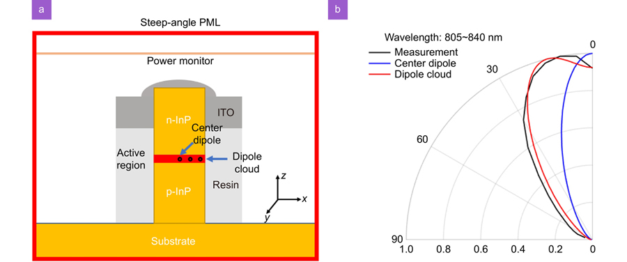
The emission wavelength of InGaN/GaN dot-in-wire LED can be tuned by modifying the nanowire diameter, but it causes mismatched angular distributions between blue, green, and red nanowires because of the excitation of different waveguide modes. Besides, the far-field radiation patterns and light extraction efficiency are typically calculated by center dipoles, which fails to provide accurate results. To address these issues, we first compare the simulation results between central dipole and dipole cloud with experimental data. Next, we calculate and analyze the display metrics for full-color nanowire LEDs by 3D dipole cloud. Finally, we achieve unnoticeable angular color shift within ±20° viewing cone for augmented reality (AR) and virtual reality (VR) displays with an improved light extraction efficiency.The emission wavelength of InGaN/GaN dot-in-wire LED can be tuned by modifying the nanowire diameter, but it causes mismatched angular distributions between blue, green, and red nanowires because of the excitation of different waveguide modes. Besides, the far-field radiation patterns and light extraction efficiency are typically calculated by center dipoles, which fails to provide accurate results. To address these issues, we first compare the simulation results between central dipole and dipole cloud with experimental data. Next, we calculate and analyze the display metrics for full-color nanowire LEDs by 3D dipole cloud. Finally, we achieve unnoticeable angular color shift within ±20° viewing cone for augmented reality (AR) and virtual reality (VR) displays with an improved light extraction efficiency.
nanowire LED microdisplay AR/VR light engines angular color shift Opto-Electronic Science
2022, 1(12): 220021
Author Affiliations
Abstract
College of Optics and Photonics, University of Central Florida, Orlando, FL 32816, USA
Conventional stereoscopic three-dimensional displays suffer from vergence- accommodation conflict because the stimulus to accommodation is fixed by the display panel and viewing optics, but that to vergence changes with image contents. With the recent rapid development of head-mounted displays, several methods have been proposed to offer the accommodation cues, among which multifocal display technology is an effective and practical solution. The first two decades of this century has witnessed the fast growth of multifocal displays from basic concept to mature implementations. This review systematically presents the state-of-the-art multifocal display design and development. Firstly, a comprehensive classification of numerous potential optical architectures to provide the multiplanar functionality is introduced, based on how the information is multiplexed and how the focal planes are generated. Next, the strengths and obstacles of reported or potential designs in each category are analyzed and compared with each other. In addition to enabling optics, the image rendering approaches for the multifocal planes are also described. This review presents a sufficient collection of past designs and is expected to offer a roadmap for future research and development of multifocal displays.
中佛罗里达大学光电学院, 奥兰多 佛罗里达 美国, 32816
Mini-LED由高密度LED二维阵列制成。它是一种全固态有源发光器件,具有工作电压低、发光效率高、响应快、性能可靠和工作温度范围宽等优点。文章结合应用讨论Mini-LED的设计和制程。
次毫米级发光二极管显示 微米级发光二极管显示 有机发光二极管显示 液晶显示 Mini-LED Micro-LED OLED LCD
美国中佛罗里达大学 光学与光电子学系, 佛罗里达 奥兰多 32816
为了研究显示器中的运动图像模糊问题, 我们推导出了一个简单的方程, 将运动图像响应时间与液晶或者有机发光二极管的响应时间以及帧率结合起来。 从方程中可以看出, 减小运动图像响应时间有3种方法: (1)减小液晶响应时间; (2)提高帧率; (3)选取合适的背光开关占空比。在显示器帧率为120 Hz时, 如果液晶的响应时间小于2 ms, 那么液晶显示器的运动图像响应时间与有机发光二极管显示器相当。液晶的响应时间可以通过两种方法提高: (1)采用超低黏性系数的液晶材料; (2)开发快速响应液晶显示器工作模式。同时, 为了使液晶显示器达到像阴极射线显像管一样快速的运动图像响应时间(< 1.5 ms), 我们可以增加帧率或者减小背光开关占空比。
运动图像反应时间 快速反应 液晶显示 motion picture response time fast response liquid crystal displays
弗洛里达中央大学, 光学与光子学院, 奥兰多, 弗洛里达 32816, 美国
自从2002年Kikuchi发现了利用稳态聚合物拓宽蓝相液晶温度范围和2008年三星展示了第一台蓝相LCD样机,整个世界对这个颠覆性技术的到来充满了期待。以克尔效应为基础的蓝相液晶技术拥有以下优点:微秒级响应时间,无需定向层,暗场时光学上是各向同性,视角大,透过率对液晶盒厚度不敏感,易于大屏制作等。对于场序性的RGB LED色彩,可以降低动态伪像,同时光学效率和分辨率可以提高3倍。然而,还有一些“瓶颈”问题需要在广泛应用之前克服,例如高操作电压、反应滞后、双折射残留和图像残留。本文将会介绍关于这些基本问题的最新进展,和一种新的具有低操作电压、高透过率、无滞后和双折射残留的蓝相LCD。蓝相液晶时代曙光将呈现在我们眼前。
蓝相液晶 克尔效应 稳态聚合物 blue-phase liquid crystal Kerr-effect stabilized polymer
1 佛罗里达中央大学光电科学学院,美国佛罗里达
2 苹果公司,美国加利福尼亚
3 全北国立大学纳米聚合物科学与技术部,韩国全州
最近,克尔效应液晶显示器由于其快速的响应时间及简单的制造工艺而受到青睐。文章通过模拟无数新兴LCD技术来了解该器件的物理原理,在提高显示器性能和优化配置方面起着重要的作用。
克尔效应 液晶显示器 蓝相液晶 Kerr effect LCD BPLC
1 美国佛罗里达州佛罗里达大学光学光子学院,美国奥兰多
2 浙江大学物理系
通过理论分析和实验研究液晶分子附着能和液晶盒间隙对响应时间(T0)的影响.用液晶盒有效间隙法和表面动力学方程法两种方法推出分析公式,由这两种方法推出的结果是一致的.实验数据与简化方程T0-dx基本拟合(其中d是液晶盒的间隙,x是指数).在两种极端的(极大或极小)附着能极限下,指数x分别接近2和1.这个结论有助于优化液晶显示器件的应用.
液晶分子附着能 液晶盒间隙 响应时间
1 佛罗里达中央大学光电子学院,美国佛罗里达奥兰多
2 陕西科技大学
研究了掺有手性分子、扭曲角为90°的垂面排列液晶盒的电光特性,该分子的手性方向与液晶扭曲方向相反.在未施加电压时,液晶指向矢呈垂面排列,但是在中间电压状态下,由于电场、表面锚定作用及反手性掺杂作用之间的平衡力矩,大量液晶分子呈垂面排列.本文着重讨论了该模式在液晶显示器方面的潜在应用.尤其是对半透半反射型双层盒的液晶显示器.
反手性分子 液晶盒 光电特性


